This is not investment advice. The author has no position in one of the shares mentioned. Wccftech.com has an disclosure and ethics policy.
An Intel Director believes that future transistor designs could make the need for advanced lithographic devices less convincing when producing high-quality semiconductors. ASMLS Extreme Ultraviolet (EUV) lithographic machines are the backbone of modern advanced chip production because they enable companies such as TSMC to print extremely small circuits on a silicon wafer. However, the Intel Director is of the opinion that future transistor designs, which include gate-all-around-fet (Gaafet) and complementary fet (CFET), are more based on the production of post-lithographic and the general importance of lithograph in the production of chips with a high end-end chips will be reduced.
Ca -etching companies can play a larger role in the future semiconductor production, says Intel Director
In a discussion published by the Investment Research Platform Tegus and was shared by X, a unnoted Intel Director announces that future transport designs will be less based on advanced lithographic devices and more on etching technology. While lithographic machines, such as the extended EUV and High-NA-E-e-e-e-e-e-e-e-e-e-e-e-e-e-e-e-eUML, the most commonly discussed chip manufacturing devices, in particular due to export control restrictions, also includes the production of a chip.
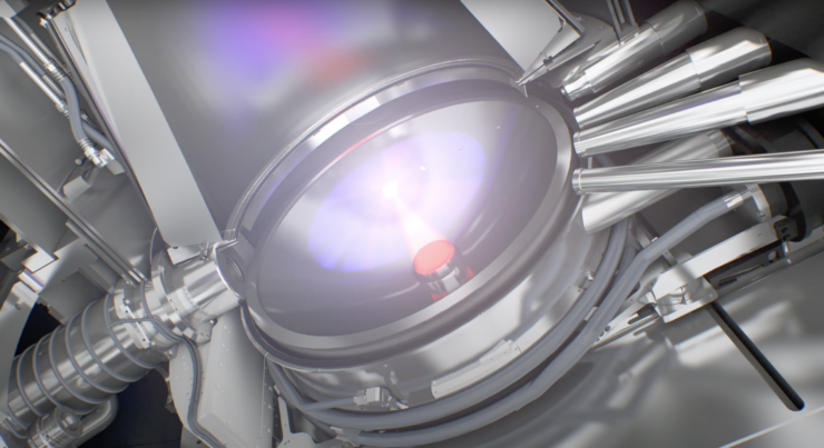
The lithograph is the first step in the process and transmits designs to the wafer. These designs are then cemented by processes such as deposition and etching. Depending on the deposit, the chip manufacturers are laid out materials on the wafer, while selectively etching to create patterns of transistors and circuits for chips.
According to the Intel Director, new transistor designs such as Gaafet and CFET can reduce the importance of lithographic machines in the chip manufacturing process. These machines, especially EUC scanners, have played a crucial role in the production of chips with 7-nanometer and advanced technologies because they can transmit or print small circuits on the wafer.
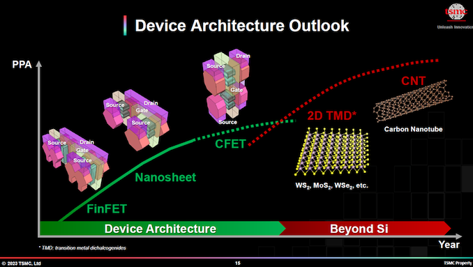
As soon as the designs have been transferred, the external material removes the excess material from the wafer to complete them. Most current transistor constructions follow the FinFet model, in which the transistors are connected to the insulating material below and get through a gate that controls the electric river in them. Newer designs such as Gaafet wrap the gate around the transistors, whereby transistor groups are in parallel. Ultra high-end transistor designs such as CFET stack the transistor groups on top of each other and save space on the wafer.
After the Intel Director it is crucial because Gaafet and Cfet “wrap” the gate from all sides. When “packaging”, the chip manufacturers have to remove excess material on the side. Instead of increasing the time that a wafer in the lithography machine spends in order to reduce the feature sizes, the manufacturers focus more on removing the material by etching.
The increasing importance of the “lateral” direction in chip production means that high NA EUV machines are “less likely” for chip production as important as its predecessors, EUV scanners, consisting of producing chips on 7-nanometer or advanced technologies. The end result of the shift is that it “reduces the dependency on the minimum function, since they can still get a high density, not only on a certain level, but also vertically,” believes the executive.
The director at Intel explains why ASML has to deal with GAA and will also fight with the move to CFETs (via Tegus). The ray of hope in relation to the order flow can later be a high NA introduction or an EUM-multiple structure in this decade, but the order flow is clearly high … pic.twitter.com/zorvjjhc2n
– Tech Fund (@techfund1) June 16, 2025