By Sandy Wen and Jacky Huang
If the dimensions shrink and the aspect ratios increase in progressive logic devices, it is becoming increasingly important to reduce the variation of the structural devices. Structural presentation variations can be a proxy for the device yield. These variations can include critical dimension (CD), Gate CD, gate height and closeness between neighboring Via.
A contribution to the variation for structural devices is mechanical deformationwhich can be caused by intrinsic material stress and thermal extent. Virtual production can help to pursue the development of voltage shaping during device production in order to understand and alleviate the effects of deformation in logic processing.
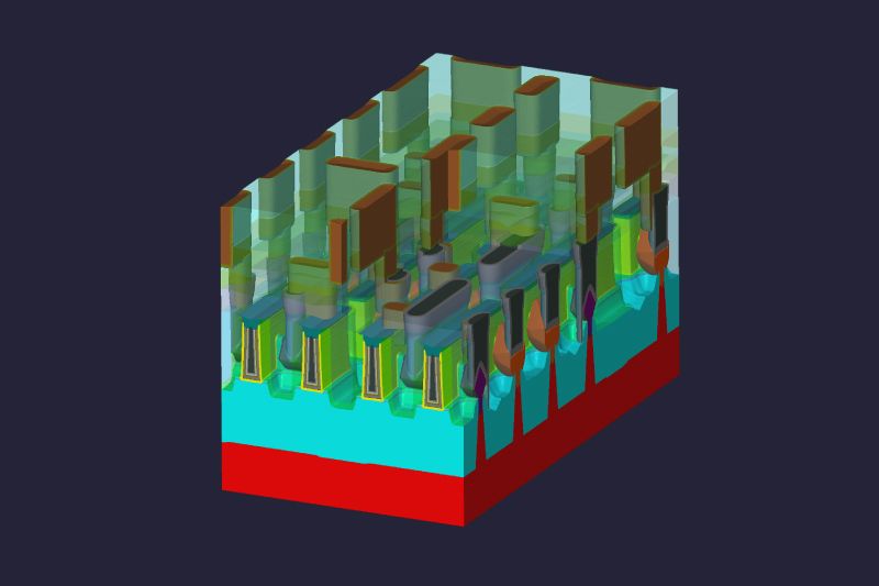
The semi-verse solution team examined stress-related deformation in an advanced FinFet process flow, which was modeled using the virtual Semulator3D platform. Deformation-related deformation was followed during the creation and removal of polysilicium-victim gate to evaluate whether these deformations would lead to process modules.

With Semulator3D, engineers can carry out virtual experiments for Finfet Sram (shown here) and other semiconductor devices.
Stress development
During the formation of Finfet gate, polysilicium is etched so that they form a sacrificial structure structure. After the formation of sources/drainage, the region that surrounds the gate is filled with dielectric material. The polysilicium structure is then removed to create a ditch that is filled with dielectric and work function metals.
The gate dimension is influenced by voltage formation during the entire wafer processing. If the intrinsic voltage of the polysilicium is varied, the gate is expanded or shrinks during the etching process due to pressure or tensile voltage, which leads to variations of the CD and gate height (Figure 1).
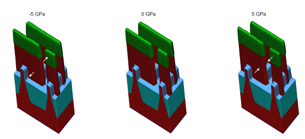
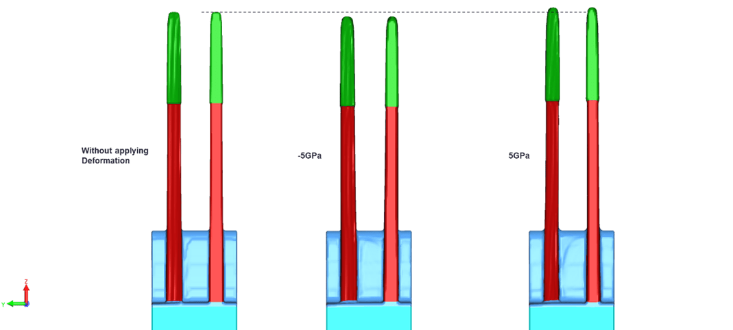
Fig. 1: Gate structure variation due to intrinsically stressed polysilicium. (Above) Gate Critical Dimension. (Below) goal height.
Later in the process flow, additional deformation occurs in the gate area, since intrinsically stressed dielectric films and tensions are in the source/drainage region between the gates.
Deformation-induced gate CD shrinkage during the nominal sacrifice removal process can leave the polysilicone rest at the end of the grave (Figure 2).
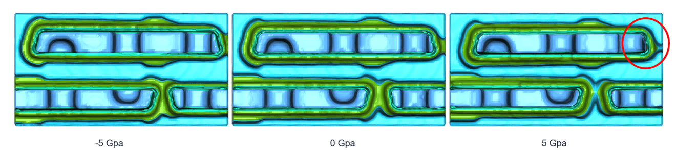
Fig. 2: If the polysilicon gate material becomes stronger, the nominal sacrificial removal process can no longer completely remove the gate material and left residues in the end of the grave.
Virtual experiments
In order to understand the effects of the tension form on the removal of the gate, two sets of virtual experiments were carried out to evaluate the process window for gate-ax and distance processes:
- One without mechanical stress awareness
- A pursuit of the development of stress deformation during processing
For each test set, the parameters were varied via several process modules to optimize the process window and achieve a given gate CD, which ensured that no polysilicium remains after the step removal step.
Study results
There was a significant difference between “in Spec %” (the success rate of achieving the specified measurement areas across all processes) for both experiment rates. Without stress awareness, the one in Spec percentage over a wide process window over 50% (Figure 3).
In contrast, More potential failures have been identified if the influence of the mechanical voltage was included in the process model. If the development of the tension formation has been included in the simulation, it decreased to less than 45%in SPEC percentage.
Therefore, we came to the conclusion that the optimal process window for this sentence of processes without considering mechanical tension cannot be achieved.
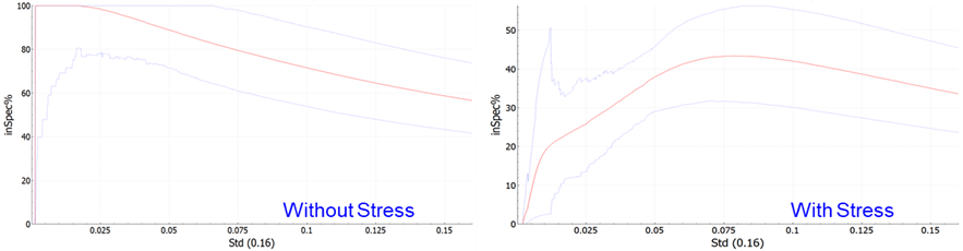
Fig. 3: For the Gate CD process window: (left) without mechanical tension awareness, the in -Spec% (red line) exceeds 50% even for larger process windows (window size). (Right) In contrast, the in -Spec% with the stress deformation development was not over 45%.
By using stress potential virtual experiments, we can get a better understanding of the effects of mechanical stress on the deformation and variation of the structure device and the determination of process windows to improve the yield performance.
The optimization of material intrinsic stress and the implementation of changes to the device structure can also be examined with stress -potential virtual production in order to limit the loss of yield induced by tension during the manufacture of semiconductor.
Jacky Huang is software engineer at Semiverse Solutions R&D Taiwan, Lam Research.
Sandy Wen
(all posts)
Sandy Wen is a Senior Staff Semiconductor Process & Integration Engineer in the Semiverse Solutions Group at LAM Research. Before that, she worked in the ETCH Business Group in various technical functions, including chamber technology and earnings improvement solutions. Sandy received her MS in EE from UCLA and BS in EECs from UC Berkeley.