

In a potential turning point for the microelectronics, scientists in Tokyo have produced a powerful new transistor that has silicon in favor of a crystalline material called gallium-doted indium oxide.
The gate design designed with a gate-all-around design, in which the tax goal of the transistor is completely around the current channel-this tiny device enriches a remarkable electron mobility and long-term stability. The result? A groundbreaking transistor that dramatically increases the performance in KI and big data applications and can keep the law of moores alive in a world after Silicon.
Transistor scaling crisis
Transistors are often referred to as one of the greatest inventions of 20TH Century. They are essential for modern electronics and act as tiny switches that control and reinforce electrical signals. But when our devices are getting faster and faster, traditional transistors struggle to keep up to keep up. Do we approach the limits of how small and powerful our electronics can become?
A team of researchers at the Institute for Industrial Science, the University of Tokyo, believes that there is a better way forward. Instead of relying on silicon, they built a new type of transistor with a material called gallium-doted indium oxide or ingaox. This special material can form a highly ordered crystal structure that helps the electrons to move more efficiently – something that is crucial for performance.
“We also wanted our crystalline oxidtranistist a” gate-all-around “structure, whereby the gate that surrounds the electricity in and off, in which the current flows,” explains Anlain, leading author of the study. “By completely changing the gate around the channel, we can improve the efficiency and scalability compared to conventional goals.”
Crystalline oxide strategy
The team started with these goals. The researchers knew that they had to introduce contamination into the indium oxide by “dying” it with Gallium. This would let the material react more cheaply with electricity.
“Indium oxide contains oxygen vacancy defects that facilitate the scattering of the carriers and thus the stability of the devices,” says Masaharu Kobayashi, senior author. “We dipped indium oxide with gallium to suppress oxygen emptying and in turn improve the reliability of the transistor.”
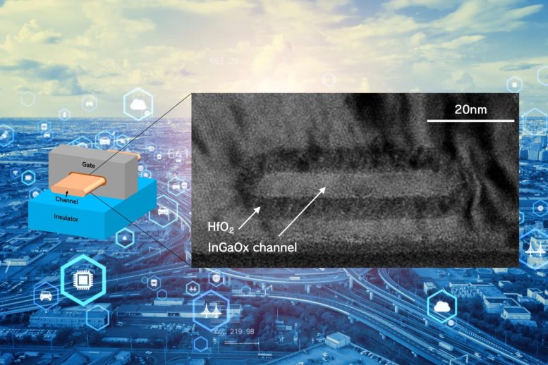
The team used nuclear shift bearing to coat the channel area of a gate-all-around transistor with a thin film by Ingaox, a nuclear layer. After the deposit, the film was heated to transform it into the crystalline structure required for electron mobility. This process ultimately enabled the production of a gate-all-around field effect transistor (MOSFET).
Gate-all-around-performance jump
“Our gate all-round mosfet, which contains a gallium-doted indium oxide layer, achieves a high mobility of 44.5 cm2/VS, explains Dr. Chen. “It is crucial that the device shows a promising reliability by being used stable for almost three hours. In fact, our MOSFET exceeded similar devices that were previously reported.”
The team's efforts have provided the field a new transistor design, which takes into account the importance of materials and structure. Research is a step towards the development of reliable electronic components with high density that are suitable for applications with high arithmetic issues, such as: B. big data and artificial intelligence. These tiny transistors promise to help the next generation technology, which makes our everyday life a big difference.
The article “A gate-all-around nano-blade oxide-necker transistor by selective crystallization of IngaoX Symposium for VLSI technology and circles was issued for performance and reliability in 2025.
Never miss a breakthrough: Join the Scitechdaily newsletter.