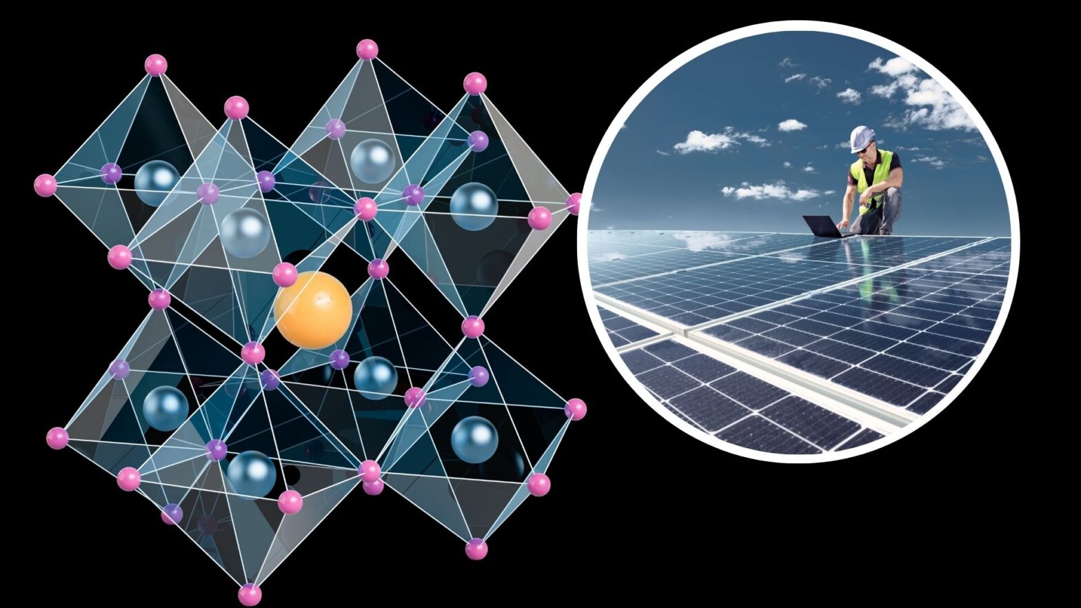
The researchers' new method, which allows greater control over halide perovskites, could transform the way solar cells, LEDs and lasers are made. Perovskites have long been touted as a potential replacement for silicon in solar cells, LEDs and quantum technologies.
The new method grows ultra-thin layers of perovskite films so that their atoms are perfectly aligned, which could enable more powerful, longer-lasting and more efficient devices.
“Much of perovskite research uses solution processing, which is messy and difficult to control,” said Professor Sam Stranks of the Department of Chemical Engineering and Biotechnology, who co-led the research.
“By switching to steam processing – the same method used for standard semiconductors – we can achieve the same level of atomic control, but with materials that are much more forgiving.”
Atomically tuned stacks
The research team used a combination of three-dimensional and two-dimensional perovskites to create and control their atomically tuned stacks, a phenomenon known as epitaxial growth. This fine control allowed the team to directly observe how the light emitted by the material changes depending on whether it is a single layer, a double layer or a thicker layer.
The researchers also found that they could design the connections between the layers to control whether electrons and holes remained together or separated – a key factor in how efficiently a material emits light.
“We have achieved a level of tunability that was not even on our radar when we started,” said Professor Sir Richard Friend of the Cavendish Laboratory, who co-led the research. “We can now decide what type of compound we want – one that holds charges together or one that pulls them apart – simply by slightly changing the growth conditions.”
The researchers found that they could adjust the energy difference between layers by more than half an electron volt and, in some cases, extend the lifetime of electrons and holes to over 10 microseconds: much longer than usual. According to a press release, this level of precision could pave the way for scalable, high-performance devices that use light in new ways, from lasers and detectors to next-generation quantum technologies.
Changing the composition and performance of perovskites
“Changing the composition and performance of perovskites at will – and studying those changes – is a real achievement and reflects the time and investment we have made here in Cambridge,” Stranks said.
“But more importantly, it shows how we can make working semiconductors from perovskites, which could one day revolutionize the manufacture of cheap electronics and solar cells.”
Published in the journal Science, the steam-based technique for growing three-dimensional and two-dimensional perovskites layer by layer, which allowed them to control the thickness of the films down to fractions of an atom.
The research could open the door to useful perovskite devices that can be manufactured on a large scale using a process like that used to make commercial semiconductors.